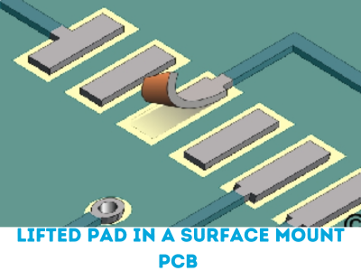
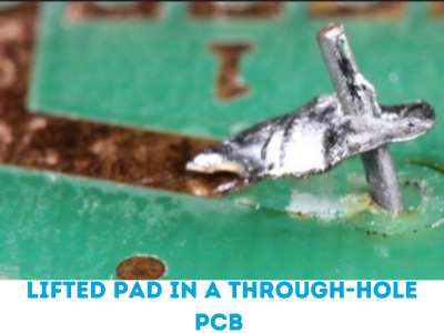
Pad lifting, a prevalent concern in PCB assembly, refers to the detachment of copper pads from the PCB substrate, often caused by excessive heat or improper handling during the soldering process.
Understanding the underlying causes, potential implications, and effective solutions for managing pad lifting is crucial for maintaining the integrity and reliability of printed circuit boards.
In this comprehensive exploration, we will delve into the root causes of pad lifting, analyze its potential impacts on PCBs, and provide practical strategies and best practices for promoting strong pad adhesion and mitigating the risks associated with pad lifting in PCB assembly.


Causes of Pad Lifting:
Pad lifting can result from various factors, including excessive heat exposure, inadequate soldering techniques, or improper PCB handling during the assembly process.
Factors such as prolonged exposure to high soldering temperatures, inappropriate soldering iron tip sizes, or the use of incompatible soldering materials can contribute to the delamination of the copper pads from the PCB substrate, compromising the structural integrity and electrical connectivity of the PCB assembly.
Impacts of Pad Lifting on PCBs:
The occurrence of pad lifting can have significant implications on the functionality and performance of PCBs, particularly in terms of electrical connectivity and mechanical stability.
Pad lifting can result in the disruption of the electrical pathways, leading to poor signal transmission, voltage fluctuations, or potential circuit failures.
Furthermore, the detachment of the copper pads can compromise the mechanical stability of the soldered components, contributing to reduced shock and vibration resistance, increased susceptibility to mechanical stress, and potential mechanical failures during the operation of the PCB assembly.
Identifying Pad Lifting:
Identifying pad lifting requires a comprehensive visual inspection of the soldered joints and the PCB substrate, focusing on the adhesion and integrity of the copper pads relative to the PCB surface.
PCBs with pad lifting issues typically exhibit raised or detached copper pads, with visible gaps or inconsistencies between the pads and the PCB substrate.
Utilizing magnification tools, such as magnifying lenses or digital microscopes, can aid in the accurate identification and assessment of pad lifting during the inspection process.
Best Practices for Managing Pad Lifting:
To manage the challenges of pad lifting and promote strong pad adhesion, implementing targeted best practices and preventive strategies is essential during the PCB assembly process.
Regulating the soldering temperature and duration within the recommended parameters specified by the solder and PCB manufacturers can aid in minimizing the risk of excessive heat exposure and the subsequent delamination of the copper pads. Ensuring the compatibility of the soldering materials with the PCB substrate and the component leads, and conducting thorough material compatibility tests, can further enhance the adhesion strength and durability of the soldered joints.
Implementing controlled cooling strategies, such as the use of specialized cooling systems or heat sinks, can aid in promoting the gradual cooling of the PCB assembly, reducing thermal stress, and minimizing the risk of pad lifting during the cooling phase.
Additionally, incorporating advanced soldering techniques, such as reflow profiling optimization and selective soldering, can provide more precise control over the soldering process and minimize the thermal impact on the PCB substrate, contributing to the prevention of pad lifting and the production of high-quality, reliable PCB assemblies and electronic products.
Conclusion:
In conclusion, comprehensively understanding the challenges of pad lifting in PCB assembly is instrumental for upholding the reliability and performance of electronic devices and systems. By addressing the root causes, assessing the implications, and adopting best practices and preventive strategies, manufacturers and electronics enthusiasts can significantly enhance the soldering quality and integrity of their PCB assemblies, contributing to the development of robust, high-functioning electronic applications and technologies.
