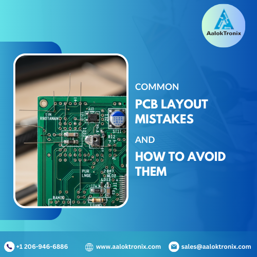
A great PCB design is much more than placing components and routing traces. Even a minor layout error can lead to overheating, EMI issues, failed prototypes, or costly production rework. Whether you’re designing a simple IoT sensor or a complex industrial controller, avoiding common PCB layout mistakes is crucial for reliability and manufacturability.
In this guide, we’ll walk through the most frequent layout errors beginners and even experienced designers encounter, and how to avoid them using best practices and Design for Manufacturability (DFM) principles.

1. What Are the Most Common PCB Layout Mistakes
Here are the errors engineers most often search for help with:
Mistake 1: Incorrect Trace Width
If a trace is too narrow for the current it carries, it will overheat, leading to burnt copper or board failure.
How to avoid it:
-
Use IPC-2152 or trace width calculators.
-
Increase copper thickness (1 oz → 2 oz for high-current sections).
-
Keep power traces wide and short.
Mistake 2: Poor Pad Spacing
Improper spacing between pads often causes solder bridging or tombstoning during assembly.
How to avoid it:
-
Follow standard footprints from manufacturers or IPC-7351.
-
Allow for enough solder mask expansion.
-
Avoid placing pads too close in high-density areas unless needed.
Mistake 3: Ineffective Grounding Strategy
Floating or segmented ground planes create noise, EMI issues, and unstable signals.
How to avoid it:
-
Use a solid, continuous ground plane whenever possible.
-
Stitch ground layers with vias.
-
Avoid splitting grounds unless necessary.
Mistake 4: Poor Via Placement
Vias directly affect signal integrity, thermal performance, and manufacturability.
How to avoid it:
-
Avoid placing vias directly on pads unless using via-in-pad technology.
-
Use multiple thermal vias under power components.
-
Separate high-speed signal vias from noisy power areas.
Mistake 5: Overlooking Component Orientation
Misaligned components slow down assembly and increase human error during inspection.
How to avoid it:
-
Keep all polarised components facing the same direction.
-
Align ICs and connectors according to assembly flow.
-
Mark all polarities clearly with silkscreen.
2. How Does DFM Help Prevent These PCB Mistakes?
Design for Manufacturability (DFM) ensures your PCB is not only functional but also easy and cost-efficient to build.
Here’s how DFM fixes layout errors:
-
Early verification of spacing, routing, and tolerances
-
Component library validation to avoid footprint mismatches
-
Thermal and mechanical checks to prevent overheating
-
Manufacturability feedback to reduce rework and production delays
At Aaloktronix, DFM is integrated into every prototype and production run, helping U.S. companies save both time and manufacturing costs.
3. What Questions Should You Ask Before Finalising Your PCB Layout?
Before releasing your files to manufacturing, ask yourself:
1. Are my traces sized correctly for the required current?
Use calculators and IPC standards.
2. Did I maintain adequate pad spacing to avoid solder defects?
Check the footprint against pick-and-place tolerances.
3. Is my grounding strategy solid and uninterrupted?
A clean ground plane improves signal integrity.
4. Are all components oriented for easy assembly?
This reduces placement errors and speeds up production.
5. Have I run a DFM review with my manufacturer?
This alone can eliminate 70%+ of production errors.
4. Conclusion
A successful PCB layout is the result of thoughtful engineering and careful planning. By avoiding common mistakes with trace widths, via placement, pad spacing, and grounding, you dramatically increase the reliability of your final product. And when combined with a professional DFM review, you reduce the risk of costly rework or prototype failures.
At Aaloktronix, we help engineers and businesses across the U.S. design, test, and produce high-quality PCBs with industry-leading precision.
???? Need help optimising your PCB layout? Get a free DFM review and PCB assembly quote from Aaloktronix today.
Let us help you build a board that performs flawlessly from prototype to production.
