
The Internet of Things (IoT) continues to revolutionise industries ranging from smart homes and healthcare to industrial automation and agriculture. While building a working prototype is an exciting milestone, successfully transitioning that prototype into high-volume manufacturing presents an entirely different set of challenges.
Many promising IoT products never reach commercial success because their PCB designs aren’t optimised for scalable manufacturing. Design flaws, inconsistent quality, supply chain issues, and inadequate testing frequently result in production delays, increased costs, and product failures.
Whether you’re developing a smart sensor, industrial controller, wearable device, or connected gateway, understanding how to scale IoT PCB assembly efficiently is essential for bringing a reliable product to market.
In this guide, we’ll walk you through every stage of the journey, from prototype validation to full-scale production, and explain why partnering with an experienced provider of PCB assembly for IoT devices is crucial for long-term success.
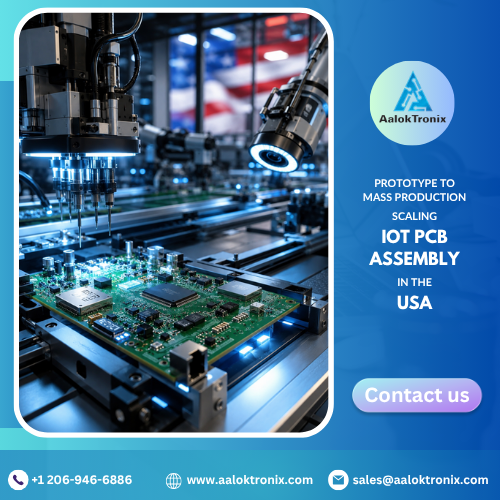
Why Scaling an IoT Product Is More Than Increasing Production Volume
Many startups assume that once a prototype works, manufacturing thousands of units is straightforward.
Unfortunately, that’s rarely the case.
Prototype boards are typically designed for proof-of-concept testing. Mass production requires entirely different considerations, including:
- Manufacturing efficiency
- Component availability
- Production consistency
- Automated assembly
- Testing procedures
- Supply chain management
- Regulatory compliance
Without preparing for these factors early, companies often face expensive redesigns before production can begin.
Stage 1: Designing a Functional Prototype
Every successful IoT product begins with a prototype.
The primary objective at this stage is validating the product’s functionality, connectivity, and overall concept.
Typical prototype goals include:
- Verifying circuit functionality
- Testing wireless communication
- Evaluating power consumption
- Confirming sensor performance
- Identifying early design flaws
At this point, flexibility is more important than manufacturing efficiency.
However, engineers should already begin incorporating design for manufacturability (DFM) principles to reduce future redesign efforts.
Stage 2: Optimizing the PCB Design for Manufacturing
Once the prototype functions correctly, attention shifts toward production readiness.
Several design improvements are typically required before moving into volume manufacturing.
Improve Component Placement
Efficient component placement simplifies automated assembly while improving thermal performance.
Poor placement can create:
- Assembly bottlenecks
- Excessive heat
- Signal interference
Following PCB layout optimization techniques helps eliminate many of these issues before production begins.
Select Production-Friendly Components
Prototype designs sometimes include components that are:
- Difficult to source
- End-of-life
- High-cost
- Available only in small quantities
During scaling, engineers should prioritize:
- Long lifecycle components
- Multiple sourcing options
- Standard package sizes
This reduces supply chain risk during mass production.
Stage 3: Choosing Materials for Long-Term Reliability
As production volumes increase, PCB material selection becomes increasingly important.
The right material directly impacts:
- Durability
- Thermal performance
- Mechanical strength
- Product lifespan
Industrial IoT devices operating in demanding environments often require advanced PCB materials.
Choosing the materials discussed in Best PCB Materials for Industrial IoT Devices in Harsh Environments helps improve reliability while reducing warranty claims.
Stage 4: Designing for Low Power Consumption
Battery-powered IoT products require careful power optimization before mass production.
Reducing energy consumption improves:
- Battery life
- Device lifespan
- Customer satisfaction
- Maintenance intervals
Key optimization strategies include:
- Sleep modes
- Efficient voltage regulation
- Low-power microcontrollers
- Intelligent firmware scheduling
These concepts are explored in greater detail in How to Design Low-Power PCBs for IoT Applications.
Stage 5: Preparing for Compliance and Certification
Scaling production also requires preparing products for regulatory approval.
Depending on the target market, certification may include:
- FCC
- CE
- RoHS
- IPC standards
Ignoring compliance until after manufacturing often leads to:
- Failed testing
- Product redesigns
- Delayed product launches
Following the recommendations in the IoT Device Certification Guide: FCC, CE & PCB Requirements can streamline approval and reduce costly setbacks.
Stage 6: Prototype Testing Before Volume Production
Before committing to full-scale manufacturing, every IoT design should undergo comprehensive validation.
Recommended testing includes:
Functional Testing
Verifies every subsystem performs as expected.
RF Performance Testing
Ensures reliable wireless communication.
Thermal Testing
Identifies overheating before production.
Applying PCB thermal management techniques significantly improves long-term reliability.
Environmental Testing
Simulates:
- High temperatures
- Moisture
- Dust
- Mechanical vibration
These tests are particularly important for industrial IoT products.
Stage 7: Identifying Reliability Risks Early
Many manufacturing problems originate long before production begins.
Examples include:
- Weak solder joints
- Poor component selection
- Inadequate grounding
- Incorrect PCB materials
- Improper trace routing
Learning from Common PCB Failures in IoT Products and How to Prevent Them allows engineering teams to eliminate these issues before they become expensive production defects.
Stage 8: Transitioning to Pilot Production
Before manufacturing thousands of units, companies typically conduct a pilot production run.
Pilot production helps verify:
- Assembly quality
- Production speed
- Testing procedures
- Yield rates
- Supply chain stability
This stage often reveals minor improvements that significantly increase manufacturing efficiency during mass production.
Working with an experienced provider of IoT PCB assembly services ensures pilot builds accurately reflect real production conditions.
Stage 9: Scaling to High-Volume IoT PCB Manufacturing
Once the pilot production run is successful, manufacturers can confidently move toward mass production.
However, increasing production volume isn’t simply about producing more boards. Every manufacturing process must be optimized to maintain consistent quality across hundreds or thousands of units.
At this stage, manufacturers focus on:
- Automated SMT assembly
- Optimized production workflows
- Consistent solder quality
- Supply chain stability
- Repeatable testing procedures
- Process documentation
- Statistical quality control
Partnering with a trusted provider of PCB assembly for IoT devices helps ensure production scales without sacrificing reliability or performance.
Stage 10: Implementing Automated Quality Control
As production volumes increase, manual inspection alone is no longer sufficient.
Modern IoT PCB manufacturing relies on automated inspection technologies to identify defects early and reduce costly rework.
Common inspection methods include:
Automated Optical Inspection (AOI)
AOI detects visible defects such as:
- Missing components
- Incorrect component orientation
- Poor solder joints
- Component misalignment
X-Ray Inspection
For complex multilayer boards and hidden solder joints, X-ray inspection provides visibility beneath components such as BGAs and QFNs.
Understanding AOI and X-ray inspection in PCB assembly helps manufacturers choose the right inspection process based on product complexity.
Stage 11: Managing the Electronics Supply Chain
One of the biggest challenges in scaling IoT products is maintaining a stable supply chain.
Electronic component shortages can delay production, increase costs, and force unexpected redesigns.
Successful manufacturers reduce these risks by:
- Approving alternate components
- Working with trusted suppliers
- Forecasting component demand
- Monitoring lifecycle status
- Maintaining strategic inventory
Planning for component availability during the design phase helps avoid disruptions later in production.
Stage 12: Controlling Manufacturing Costs
Scaling production should improve efficiency, not dramatically increase costs.
Several factors influence manufacturing expenses, including:
- PCB complexity
- Layer count
- Material selection
- Component availability
- Assembly time
- Testing requirements
- Production volume
Engineers can better estimate budgets by understanding PCB manufacturing cost factors.
Optimizing the design before production often reduces overall manufacturing costs while improving yield.
Why Many Companies Choose IoT PCB Manufacturing in the USA
While overseas manufacturing may appear cost-effective initially, many companies are choosing USA-based PCB assembly for faster turnaround, improved communication, and greater quality control.
Benefits include:
Faster Prototyping
Shorter shipping distances enable quicker design revisions and faster product launches.
Improved Quality Assurance
Working closely with domestic manufacturing teams allows faster issue resolution and stronger quality oversight.
Better Intellectual Property Protection
Manufacturing within the United States often provides additional confidence for companies developing proprietary technologies.
Simplified Logistics
Domestic production reduces shipping complexity and minimizes delays caused by international supply chain disruptions.
These advantages are particularly valuable for startups, medical device manufacturers, aerospace companies, and industrial IoT developers.
Common Mistakes When Scaling IoT PCB Production
Many organizations underestimate the complexity of moving from prototype to production.
Some of the most common mistakes include:
Ignoring Design for Manufacturability
Prototype designs often require modifications before they can be efficiently manufactured.
Applying design for manufacturability (DFM) principles early helps avoid costly redesigns.
Selecting the Wrong PCB Materials
Choosing low-cost materials without considering operating conditions can significantly reduce product lifespan.
Selecting materials discussed in Best PCB Materials for Industrial IoT Devices in Harsh Environments helps improve durability and long-term performance.
Overlooking Thermal Performance
As production volumes increase, even minor thermal issues can become widespread field failures.
Implementing PCB thermal management techniques improves reliability across every production batch.
Delaying Compliance Planning
Waiting until the product is complete before considering certification often results in project delays.
Preparing early using the recommendations in IoT Device Certification Guide: FCC, CE & PCB Requirements simplifies regulatory approval.
Insufficient Testing
Skipping validation to reduce costs often results in expensive warranty claims later.
Manufacturers should combine:
- Functional testing
- Environmental testing
- Burn-in testing
- AOI
- X-ray inspection
to maximize product reliability.
Building Reliable IoT Products for Long-Term Success
Scaling from prototype to mass production requires careful coordination between engineering, procurement, manufacturing, and quality assurance teams.
Successful IoT manufacturers focus on:
- Design optimization
- Reliable materials
- Manufacturing consistency
- Regulatory compliance
- Comprehensive testing
- Continuous quality improvement
These practices reduce production risks while improving customer satisfaction and product longevity.
Whether you’re producing hundreds or hundreds of thousands of IoT devices, every stage of the manufacturing process contributes to the final product’s success.
Final Thoughts
Developing a working prototype is only the beginning of the product journey. Successfully scaling to mass production requires thoughtful planning, robust design practices, reliable supply chains, and experienced manufacturing partners.
By incorporating design for manufacturability, selecting appropriate PCB materials, optimizing power efficiency, performing rigorous testing, and planning for compliance early, companies can confidently transition from prototype builds to high-volume production.
At Aaloktronix, we specialize in PCB assembly for IoT devices, supporting businesses across the United States with prototype development, pilot production, and scalable manufacturing solutions. From concept to commercialization, our experienced team helps ensure every IoT product is built for quality, reliability, and long-term success.
Ready to scale your IoT product? Contact Aaloktronix today to discuss your PCB assembly and manufacturing requirements.